Defining Goals :
- Make a PCB board using KiCad
- Play around with the design to make it look more expressive, shaped like a cat for example
-
Note : learning arduino helps with prototyping, you can create your prototype to understand which components you need for your project as well as how to connect them. Then you can take the prototype and recreate it in kicad.
After watching the video from the electronics design week and getting familiarized a little bit with the different components and what they do.
Some of the components mentioned :
- Ribbon Cable (wires in a ribbon) and is graded by what is called AWG which refers to the gauge of the diameter. Gauge is a measure of the size of a wire which correlates with how much current you can put through the wire.
![]()
-
IDC Connector
- Slide Switch can be used as a configuration switch or a low power switch.
- Resistor used for limiting the flow of current
- Capacitor used for local charge storage
- Polarized capacitors is a component that is been a capacitor and a battery, they can store large amounts of power
- Crystal/Resonator are used to determine time. Mainly used to determine high resolution timing/high accuracy
- Inductor when a current flows through it, it creates a magnetic field
- Diods the current can go only in one direction. There are two sides to the diod, one is called anode and the other cathode
- LEDs are a particular kind of diod. LEDs have a particular indication for direction. For instance, if you see a green line on one side and it is on the cathode side. You always use an LED with a current limiting resistor and the resistor will determine how bright the LED is going to be
- Transistor there are bipolar ones, which we are not going to use. Mosfits are one of the key components in the class, there is a P mosift (source of current) and an N mosfit(sink of current). There is a drain and a source on one side and the gate on the other. RDS is the resistence between the drain and the source. Both are used to control things that take a lot of current like motors or speakers.
- Regulators are regulated by current input voltage and output voltage. You need a capacitor on the right side
- Amplifiers are now built into the processor, you can pick them in software and you don’t need a seperate component.
- Micro-controllers are a world of their own, there is so much to cover and learn about.
Circuits!
I figured I should first familiarized myself a little bit with circuits so I watched a few videos explaining Ohms law. I already got an introduction to electricity thanks to the arduino course, there are more videos to watch yet I will revisit them later.
Drawing circuits is called EDA which stands for electronics design automation The drawings need to be hirarchical and parametric There are footprints Kirchhoff’s current law
REFDES which stands for reference designator is a combination of numbers and letters used to identify electrical components on a board.
Learning kicad
As an excerise I followed along an intro to Kicad Series on youtube. I created a local library and created a symbol inside of it.
Note: Putting the datasheet & the schematic desing side by side can be useful
Steps :
- First, I installed the fab academy library which can be found on the electronics design week and added it to kicad.
https://gitlab.fabcloud.org/pub/libraries/electronics/kicad
- Go to preferences > Manage Symbol Libraries
- This will open symbol library > add “fab.kicad_sym” there
- Go to preferences > Manage Footprint Libraries
- Add “fab.pretty” there
- Go to preferences > Configure Paths and add variable named FAB that points to the installation directory of the fab library as in where you saved the library on your computer.
Starting a new project
- File > new project
- Name your project and save it in a suitable folder
- Two files will pop up on the left side > the schematic file & a blank pcb file
https://www.youtube.com/watch?v=c2niS9ZRBHo
Running the library editor
-
Go to tools > symbol editor and press ok to load the library
-
File > new library > project > local and create a new library for the components
-
Note if you want to store your component in a larger library that is accessible by all your projects you can choose global. The advantage of having your library assigned to a project specific (local) is that it becomes easier to share your custom parts if you were to upload your project to say something like GitHub
-
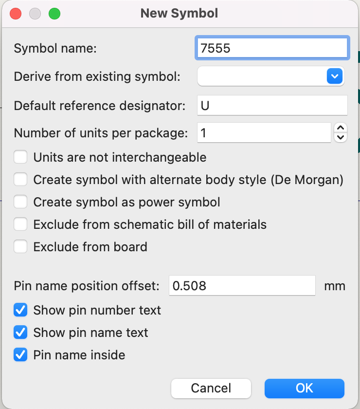
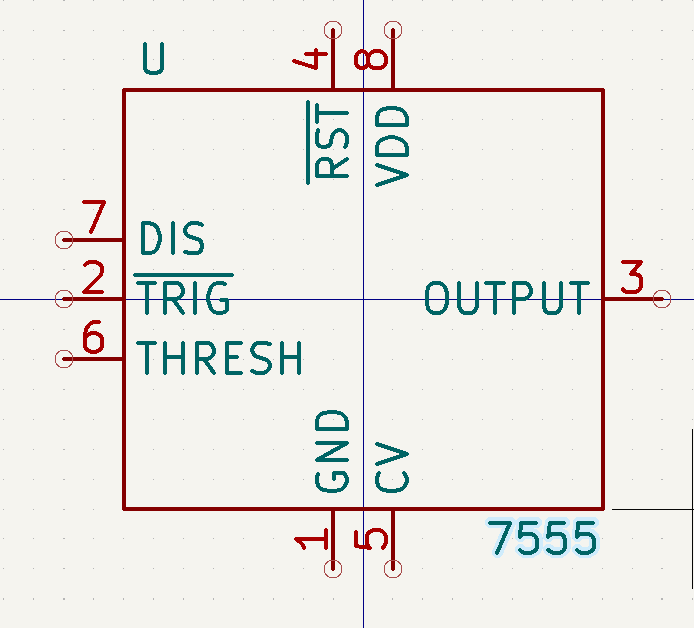
Add a new symbol : following the tutorial, the component was named as 7555 which is an intigrated circuit derived from 555 made back in the 70s. The older version was made with bipolar transistors intended for things like oscillators and pulse generators. The 7555 works just like the 555 but instead of bipolar transistors, it uses CMOS. CMOS can operate at lower voltages, for our project it will be powered by a 3 volt coin cell battery
-
Google the reference designator. There we can see that intigrated circuits like our example 7555 is referenced by the letter U
-
Save it!
-
Click the add pins button and add GND, number 1 following the datasheet and do the same for the others. Keep in mind that the way to name active low pins is by typing ~{NAME}
-
Look at the Data Sheet for specifics
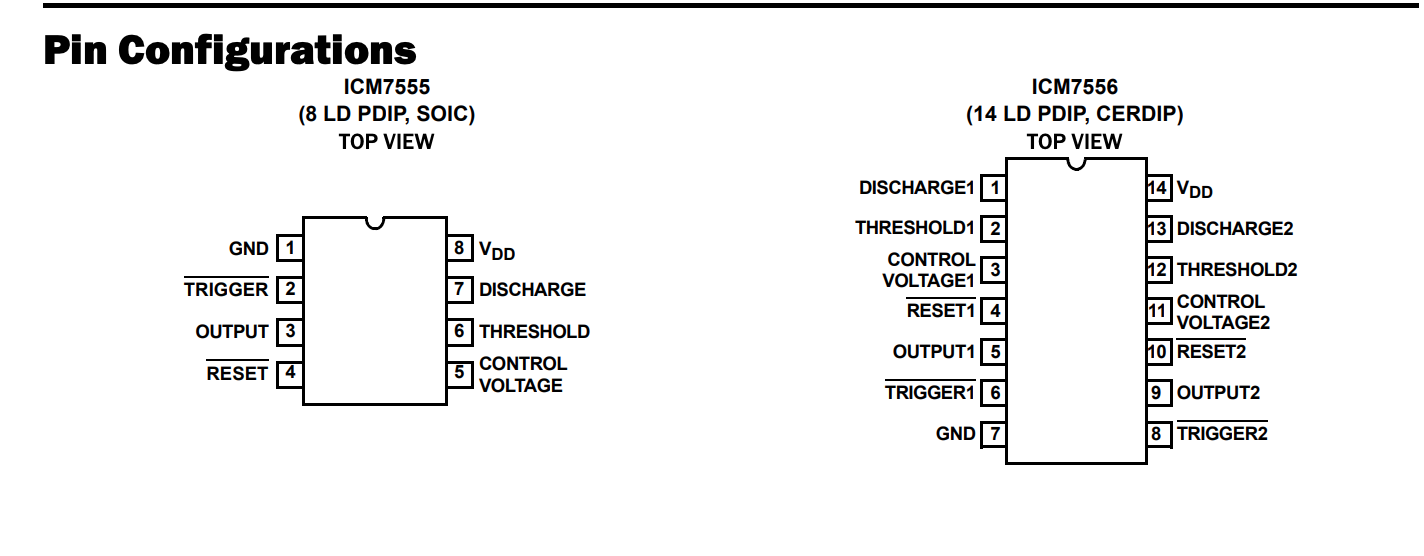 Active low pins are specified by the dash on top of the name
-
Advice putting the datasheet and the library editor side by side can be helpful
-
Then go to http://www.555-timer-circuits.com/flashing-led.html and keep this schematic next to your library editor in order to know how to place your pins. Using move and rotate (r on keyboard) fix them accordingly
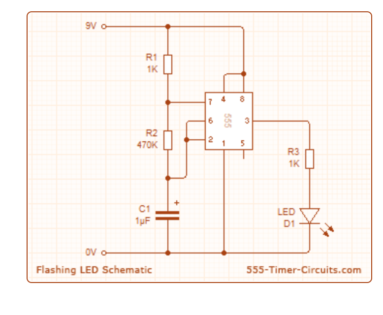 Add a rectangle around it once you are done!
- At the end of this part, you should have this schematic
Schematic Capture/Editor
- Some information: the numbers and letters in between the boarders are a way to refer to sections. For instance you could refer to an issue located at b4 and other engineers can know where to look.
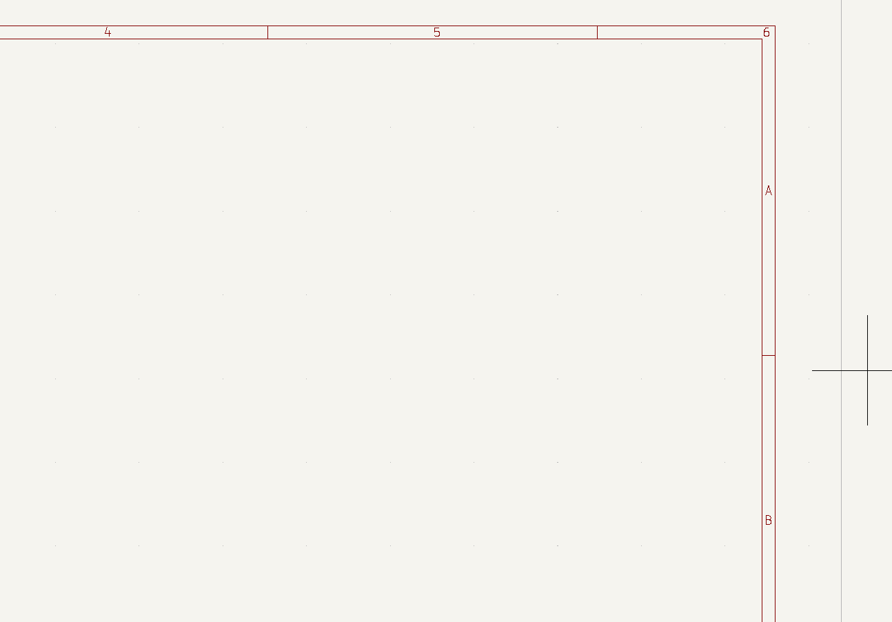 Section b4
-
Bottom right contains information about your schematic, similar to autocad basically. To fill this part out in case you want to share your schematic or keep track of changes go to file > page settings
-
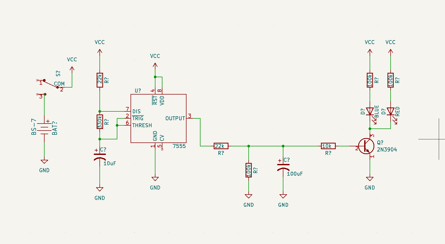
Go to place > add symbol and choose the symbol we created. Alternatively you could press A on your keyboard. Then do the same and add 3 basic resistors. Remember that is where the arduino prototype comes in handy you just add the components based on your prototype and then connect them accordingly!
-
double click on R and rename according to the resistors used, 2 are 22k in our example, 10 k, 3 are 100k, 330k
- Then we repeated the same process, for 2 capacitors and name one 10uF and the other 100uF
- Then again for the LEDs (2) rename RED
- Then lastly a transistor 2N3904
- Kicad doesn’t have a battery holder or slide switch that we need for our board, so we can use a third party such as digi-key. So we got it from github.com/digikey/digikey-kicad-library repeat the same process as we have done for the fab library. Add this specific library from the file : dk_Battery-Holders-Clips-Contacts.lib and **
- Press a on your keyboard and select BS-7 battery from the new library you just added! Do the same for the slide switch EG1218
- Adding Flags helps, as it adds the effect of connecting things together without having to look at wires on the screen.Any node with a flag name is automatically connected to other nods with the same flag &name. Powering ground flags on schematics & VCCs (basically all the components wired to a common ground o vcc)
- Add wires start with the GND on the far left and connect it to the negative battery pin, this tells Kicad that we intend for the negative battery terminal to be connected to all the other GND node pins
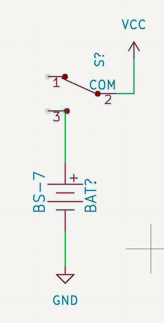 Wires connected on the left side
Completed schematic plan
Create a footprint in KiCad
(Most probably won’t need to do that but thought I’d go along with the tutorial and learn it anyways!)
- Open the INTERSIL datasheet
- Go to tools > create footprint
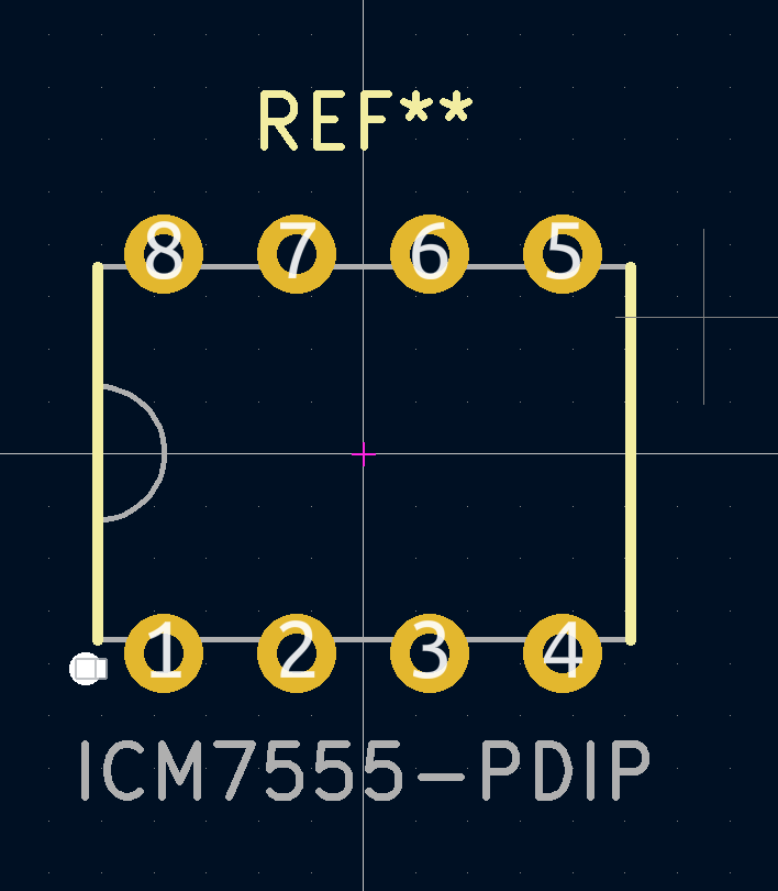
- File > new footprint and name it as ICM7555-PDIP as that will assoiciate it with the exact part from the intersil datasheet! and shows that we are using the plastic dual in-line package
- File > new library > local > make sure it is in the folder of your project and name it as 555_Badge. Note that .pretty stands for footprint library
- Preferences > manage footprint libraries and you will see that it is associated with the footprint library you just created
- Units, when it comes to PCBs some datasheets will give you data in mm and others will give you data in inches and some will give them to you in both.
- Create pads, go to place > add pad then right click to give it a number and position it correctly. For the pad type choose through hole and choose circle for the pad shape as well as hole shope. Choose 0.03 for the hole size. Pad size in inch is 0.06. The specifications can be found on the datasheet! Always go for the max just to leave room for mistakes
- Outline Click place > line, double click on the line to edit it. The thickness 0.004, start point 0.2 for x and 0.14 for y and end point 0.2 for x and - 0.14 for y, choose F.Fab layer
- On the right side, click on F.Fab to change our layer, then add an arc in the middle, click and on the bottom you will see the x and y coordinate, press space to add a relative distance click at -0.2 and zero then click again at -0.2 and -0.05.Then edit its properties and make sure the angle is 180, also change the line thickness to 0.004
- then add two vertical lines on top of the lines we have with thickness of 0.008 on layer silkscreen
- Then add a small circle on the left bottom side with the width of 0.008
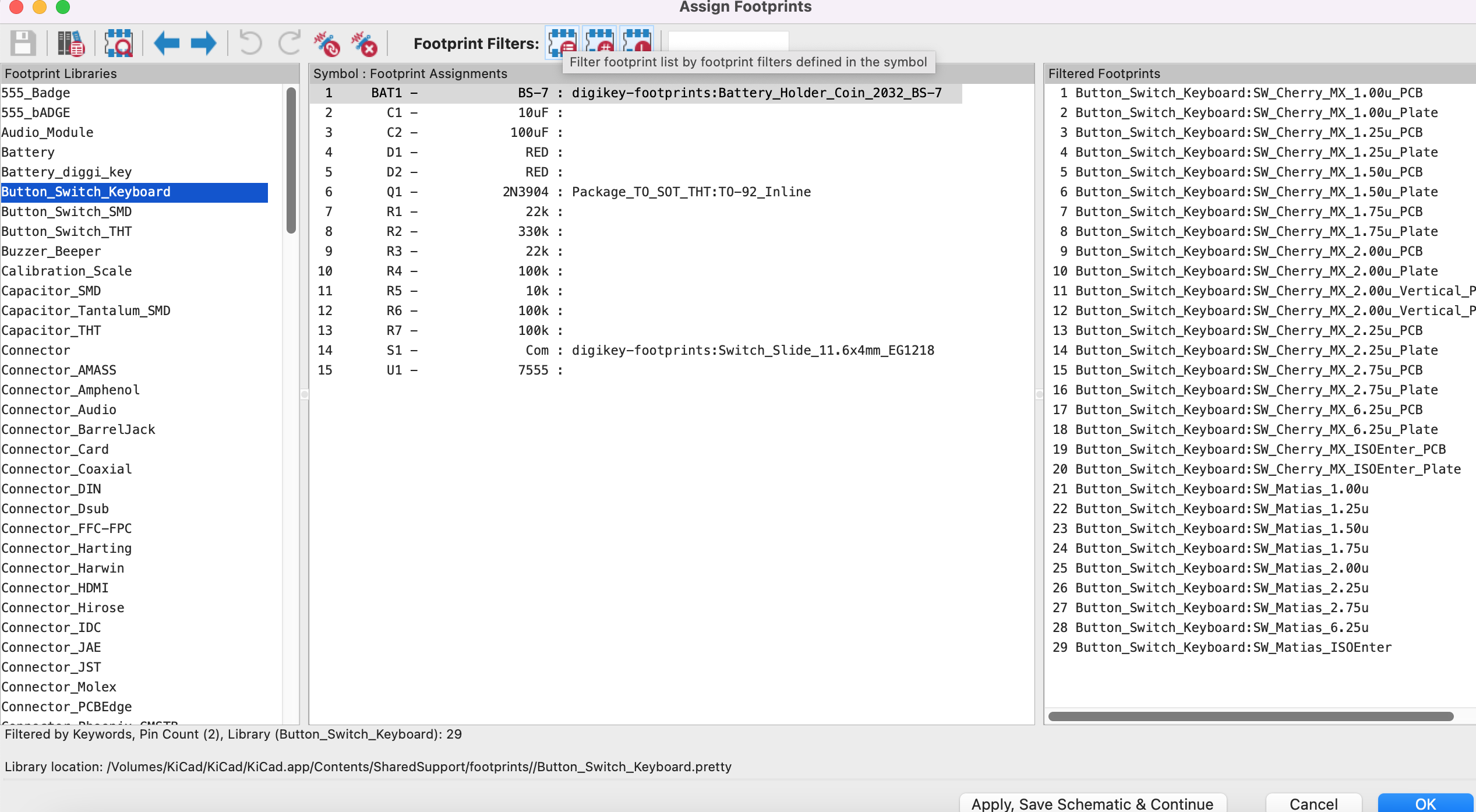
Associate Footprints and Generate Netlist
- First press on run footprint assigment tool it will replace all the ? marks with numbers
- Go to preferences > manage symbol libraries and check if you have the global ones loaded
- Go back to the runn footprint assigment tool, in there click preferences manage footprint libraries
- Go to github.com/kicad and download the foot print reposotory and save it in the libraries folder, make a new foder there called kicad and add it there.
- Add the footprint library from kicad reposotory as well as the digi key footprint one
- on the left side you will see the new libraries loaded
- You can filter footprints based on keywords or pin count or according to footprints available in a specific library
-
Do some research on the type of capacitor needed, we know that we want it to be aluminum electrolytic capacitor, through hole with 10uf, select those filters. on digi-key.com search for capacitor and add those filters
-
There are two types of through the hole parts : radial(extend from the radius of the cylinder) or axial(extend from the main axis of the cylinder)
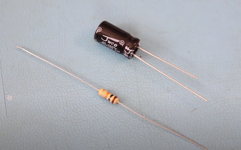
- We are looking for a capacitor that is THT(through the hole) with a radial, 5 mm and pin spacing of 2 mm
- Repeat same process for the capacitor with the 100uf (research, fine, attribute)
- For the LED also through hole, D3.0
- Resistor
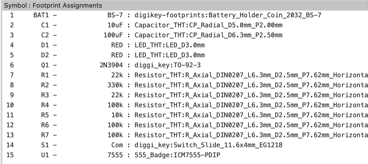 All the assigned footprints
- Save!
Place parts and define Outline
- File > page settings (fill it out the same as we did with the schematic)
- Be mindful of units
- Tools > update pcv based on schematic
- Head to https://oshpark.com/ to find information about the board we are making. There go to support > see all docs > KiCad > Manually set the design rules
- It would be helpful to put the design rules and the kicad folder side by side
- Go to file > board Setup > Solder Mask/Paste to determin Solder Mask Clearance how much space there should be between the pad and the start of the solder mask, check the specifications on the website, 0.002
- Design Rules make sure do not allow micro vias is selected
- Via is like a through-hole(yet they are much smaller) in the board where the copper and substrate layers are drilled, copper is added using an electroplating process. They connect copper or traces between layers. Uvia stands for micro via. Make Clearance & track a little bit bigger than the board houses minimum specifications, 0.01. Via diameter 0.03 and drill to 0.015
- Move all parts so they are not piled on top of each other, the wire connecting them are called air wires they are helpful in figuring out how parts should be connected with traces. The entire group of air wires is known as ratsnest because it looks like a ratsnest
- Show boards ratsnest to toggle between switching on and off the ratsnest
- For drawing an outline move to the Edge.Cuts layer and select a line